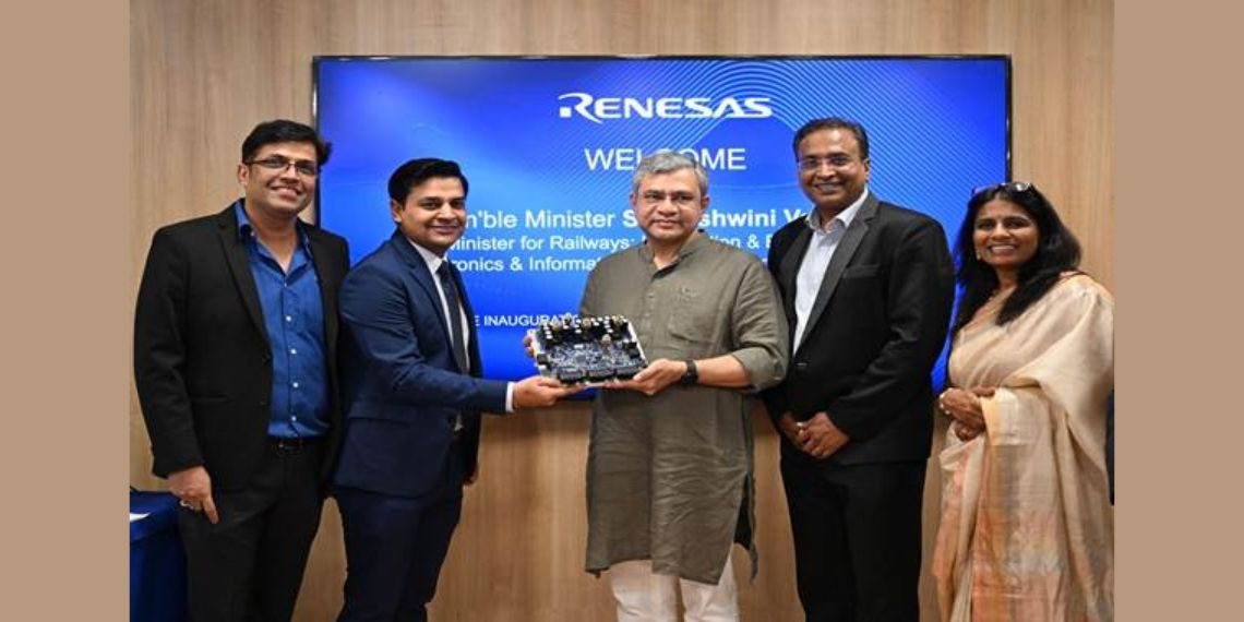
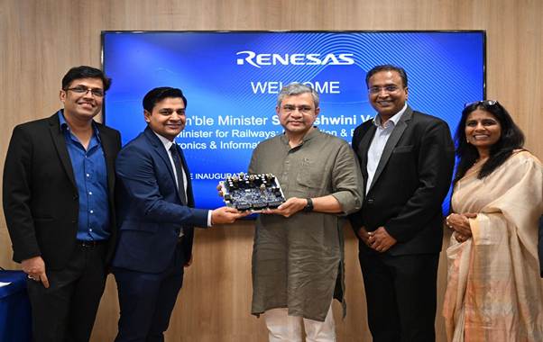
India has reached a critical milestone in its semiconductor journey with the launch of the country’s first-ever 3-nanometer (3nm) chip design centers. In a significant development for the tech and electronics sector, Union Minister for Electronics, Railways, and Information & Broadcasting, Ashwini Vaishnaw, inaugurated two Renesas Electronics India design facilities in Noida and Bengaluru. This move strengthens India’s ambition to emerge as a global semiconductor powerhouse.
Key Highlights
India’s first 3nm semiconductor design centres launched
Developed by Renesas Electronics India in Noida and Bengaluru
India transitions from 7nm and 5nm designs to advanced 3nm nodes
Focus on talent development through academic collaborations and new hardware kits
Support from the India Semiconductor Mission (ISM) and strategic Indo-Japan partnerships
A New Chapter in India’s Semiconductor Journey
The inauguration of these advanced chip design centres marks India’s entry into the elite league of nations working on 3nm semiconductor technology. While India has previously contributed to the development of 7nm and 5nm chips, this shift to 3nm represents a significant technological leap. As Ashwini Vaishnaw stated during the inauguration, “India has worked on 7nm and 5nm designs before, but 3nm sets a new standard.”
The new facilities are operated by Renesas Electronics India, a leading global player in embedded semiconductor solutions. These centres will drive innovation in high-performance computing and low-power chip designs, supporting applications in automotive, industrial, and IoT domains.
About Renesas Electronics: A Strategic Partner for India
Renesas is renowned for its expertise in embedded systems and system-on-chip (SoC) design. Its core portfolio includes:
High-Performance Computing
Embedded Processing Solutions
Analog & Connectivity Components
Power Management Systems
Renesas has ramped up its India operations, with active design hubs now in Noida, Bengaluru, and Hyderabad. These centers will play a vital role in developing next-generation chips for global markets.
Government Vision: Building a Comprehensive Semiconductor Ecosystem
Vaishnaw emphasized that the launch aligns with India’s long-term semiconductor strategy, which involves:
Advanced chip design and fabrication
Establishing ATMP (Assembly, Testing, Marking & Packaging) units
Creating supply chains for semiconductor equipment, gases, and chemicals
The Minister noted growing international confidence in India’s capabilities, backed by major investments from global firms such as Applied Materials and Lam Research.
He also highlighted Noida’s role as a pivotal node in India’s national semiconductor infrastructure, stating, “India’s skilled workforce and robust academic institutions are the foundation of our global ambitions.”
Strengthening Talent Through Semiconductor Education
To ensure a sustainable pipeline of skilled professionals, the government has launched initiatives to enhance semiconductor education in India. One major highlight is the distribution of semiconductor learning kits to over 270 academic institutions.
These kits offer students:
Hands-on hardware training
Access to industry-grade EDA software under the India Semiconductor Mission
A blended learning experience that integrates both hardware and software design skills
Vaishnaw credited CDAC and the India Semiconductor Mission team for accelerating talent development. “We are preparing engineers who can contribute from day one in global semiconductor projects,” he said.
Vision for Growth Under Aatmanirbhar Bharat
The push for advanced semiconductor capabilities is deeply embedded in the larger Aatmanirbhar Bharat (Self-Reliant India) vision spearheaded by Prime Minister Narendra Modi. According to Vaishnaw, the sector has evolved rapidly within just three years — from nascent beginnings to becoming an emerging global hub.
The demand for semiconductor chips is expected to rise exponentially across:
Smartphones and Consumer Electronics
Data Centers and Cloud Infrastructure
Medical Devices and Healthcare Systems
Defense and Aerospace Equipment
Electric and Connected Vehicles
India’s efforts are designed to meet this demand both domestically and globally, reinforcing its role in the global supply chain.
Renesas’ Continued Commitment to India
Renesas CEO Hidetoshi Shibata reaffirmed India’s strategic importance to the company’s global roadmap. He highlighted:
A vision for end-to-end chip design, testing, and innovation
Strong support for over 250 academic institutions and startups through government-backed programs like Chips to Startup (C2S) and the Design Linked Incentive (DLI) scheme
Leveraging India’s engineering talent pool and the Indo-Japan partnership to reshape the global semiconductor landscape
Shibata expressed confidence that India would play a defining role in shaping future technology innovation across embedded systems and intelligent hardware.
Conclusion:
The launch of India’s first 3nm chip design centres is a landmark achievement that signals a new era of advanced electronics design and innovation. Backed by global collaboration, government support, and a growing talent ecosystem, India is swiftly moving towards becoming a key player in the global semiconductor value chain. With the foundations now in place, the future looks promising for India’s digital and technological leadership.
Follow Before You Take on:
Latest Technology News | Updates | Latest Electric Vehicle News | Updates | Electronics News | Mobile News | Updates | Software Updates
📌 Facebook | 🐦 Twitter | 📢 WhatsApp Channel | 📸 Instagram | 📩 Telegram | 💬 Threads | 💼 LinkedIn | 🎥 YouTube
🔔 Stay informed, Stay Connected!